
- About
- Apply
- Awards + Funding
- Graduate Students
- Life + Community
- Faculty + Staff
- Individualized Interdisciplinary Studies in Graduate Studies
"Considering SFU’s reputation for science and technology, and its excellence in this field, pursuing graduate studies at SFU is a unique privilege."
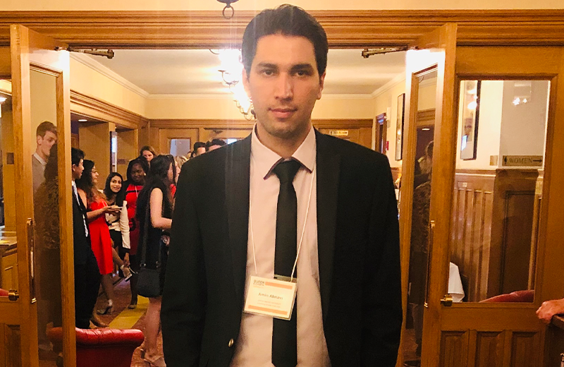
Amin Abnavi
doctoral student in the Faculty of Applied Sciences
I’m a PhD student in the School of Engineering Science (ENSC) at SFU. I grew up in a beautiful farming village named Tir Taj, Doshmanziari district, Fars province, Iran. My interest in science dates back to school days, when I was fascinated – and still am, in a way – in front the household television set, my grandmother’s radio set and my little rechargeable car. Growing older, I studied Electrical Engineering and Electronics, driven by the hope that my modest contribution in this field could have an impact on our daily lives. During my undergraduate studies, I learned mainly about electronic devices, electrical and communication circuits, but I have always felt drawn to study electronic devices at the atomic level. I therefore pursued my studies in Semiconductor Technology, focusing on the fabrication of electronic components and nanoelectronics devices. The challenges are far from being only scientific or academic: I also firmly believe that advances in the field of nanoelectronics devices can help tackle major issues like pollution and global warming, by contributing to develop high-performance, and self-powered electronic and optoelectronic devices.
WHY DID YOU CHOOSE TO COME TO SFU?
Considering SFU’s reputation for science and technology, and its excellence in this field, pursuing graduate studies at SFU is a unique privilege. I was particularly interested in the research carried out by the Nano-device Fabrication Group, led by Dr. Michael Adachi, that has been focusing on fabrication of 2D material-based electronic devices and flexible Si hetero-junction solar cells.
HOW WOULD YOU DESCRIBE YOUR RESEARCH OR YOUR PROGRAM TO A FAMILY MEMBER?
From the devices we are using in our daily lives to the very high-tech instruments in huge organizations such as NASA, there is one essential component: the processor! Silicon wafers are the building blocks of today’s processors. Advances in silicon have been tremendous and have pushed silicon transistors and circuits to their limits. Lately, researchers across the globe found out that some atomically thin 2D materials have outstanding electrical, optical, and mechanical properties, making them even more suitable for such processors. Our research is to develop next-generation electronic and optoelectronic devices based on these new materials to have faster, smaller, and more efficient processors.
WHAT ARE YOU PARTICULARLY ENJOYING ABOUT YOUR STUDIES/RESEARCH AT SFU?
I’m enjoying working with my supportive supervisor, Dr. Michael Adachi, my excellent research collaborator, Ribwar Ahmadi, and my friendly lab mates. I’m also enjoying the multicultural, positive, and supportive atmosphere at SFU.
HAVE YOU BEEN THE RECIPIENT OF ANY MAJOR OR DONOR-FUNDED AWARDS? IF SO, PLEASE TELL US WHICH ONES AND A LITTLE ABOUT HOW THE AWARDS HAVE IMPACTED YOUR STUDIES AND/OR RESEARCH.
I have been fortunate enough to be selected as the recipient of the following awards: - The Canadian Queen Elizabeth II Diamond Jubilee Scholarship, 2019-2020 - Lang Wong Memorial Endowment Scholarship in Engineering, 2019 & 2021. - Kaiser Foundation for Higher Education Graduate Scholarship, 2020 & 2021. These awards have helped me a lot to focus solely on my field of interest without having to worry about the high cost of living in Vancouver.
HOW WOULD YOU DESCRIBE YOUR PROGRAM/POSTDOC POSITION TO SOMEONE STILL SEARCHING FOR A PROGRAM OR POSTDOC POSITION?
Recently, the semiconducting 2D layered transition metal dichalcogenides (TMDCs) have been widely reported for their unique electrical, optical, mechanical, and chemical properties, which vary from bulk to monolayer. Moreover, TMDCs materials show excellent potential for widespread applications such as photodetectors, light-emitting diodes, solar cells, memory devices, resonators, and biosensors. At the Nano-device Fabrication Group, we are working on the development of high-performance, flexible, and thin electronic and optoelectronic devices using these 2D materials.
IS THERE ANYTHING ELSE YOU'D LIKE TO SHARE?
Outside of the lab, I enjoy hiking, biking, and swimming.
Contact : aabnavi@sfu.ca