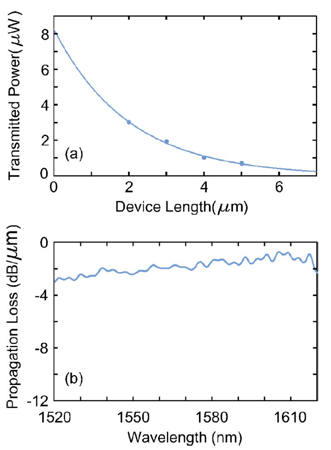
Abstract
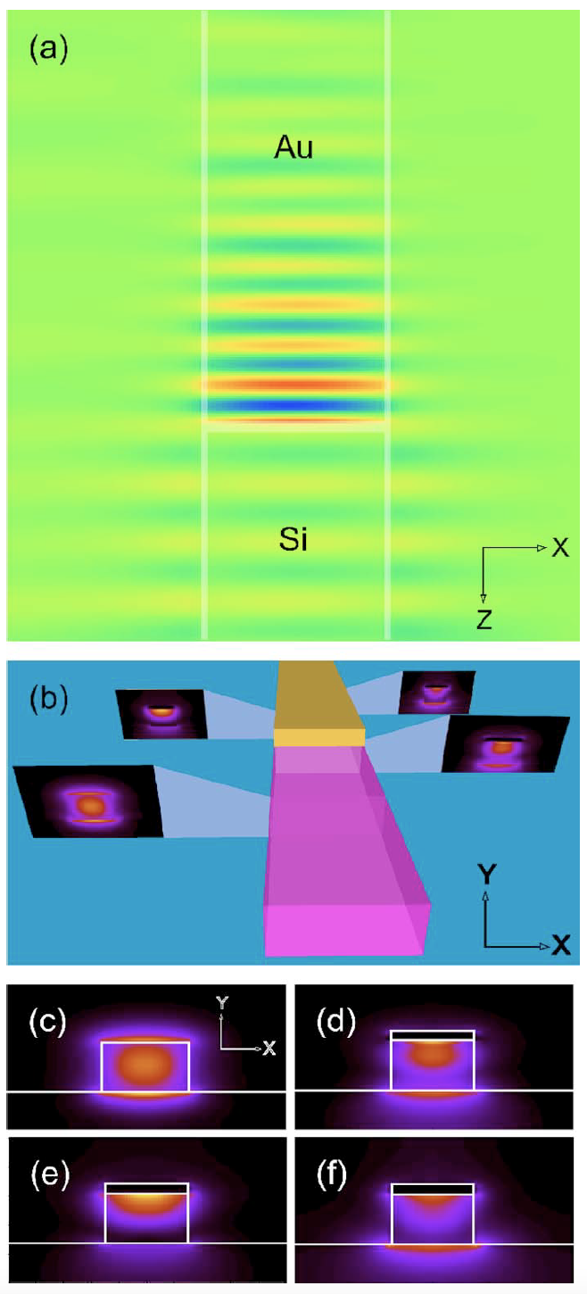
A silicon-based plasmonic waveguide was designed and fabricated for use at telecommunications wavelengths. This waveguide is interfaced to the silicon photonics platform by use of a tapered silicon-on-insulator waveguide. Simulations indicate that this scheme excites the transverse magnetic plasmonic mode and that the electric fields are confined to the silicon-gold interface. Transmitted power is measured for several device lengths and the propagation distance and coupling efficiency are found to be 2.00 μm and 38.0%, respectively. These results demonstrate the potential for integration between silicon photonics and silicon plasmonic devices and demonstrate the ability to incorporate silicon-based plasmonic devices into complimentary metal-oxide-semiconductor electronic and photonic circuitry.