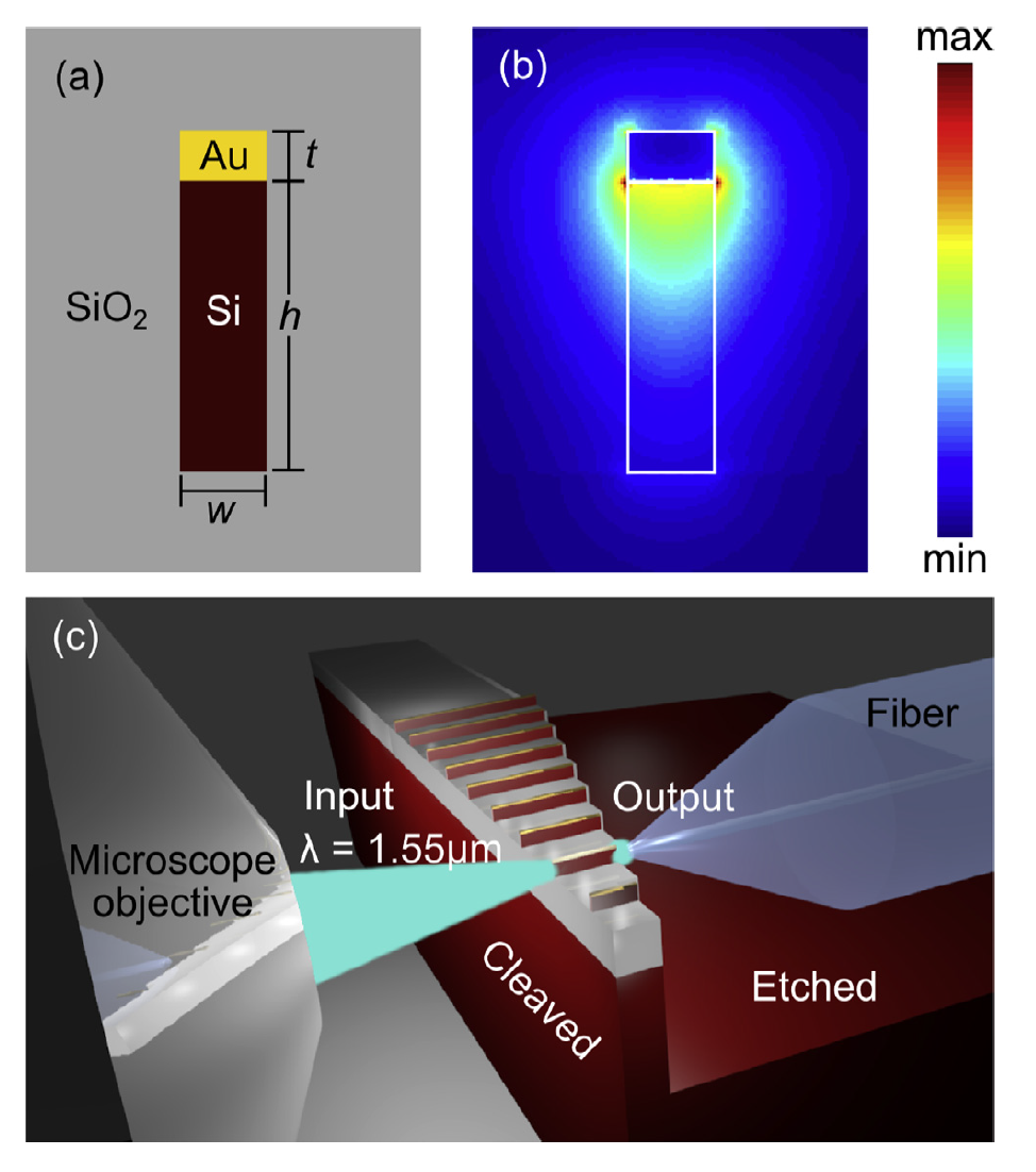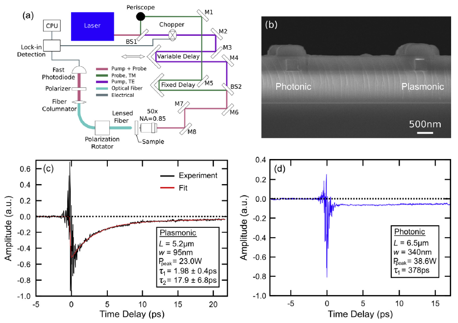
Abstract
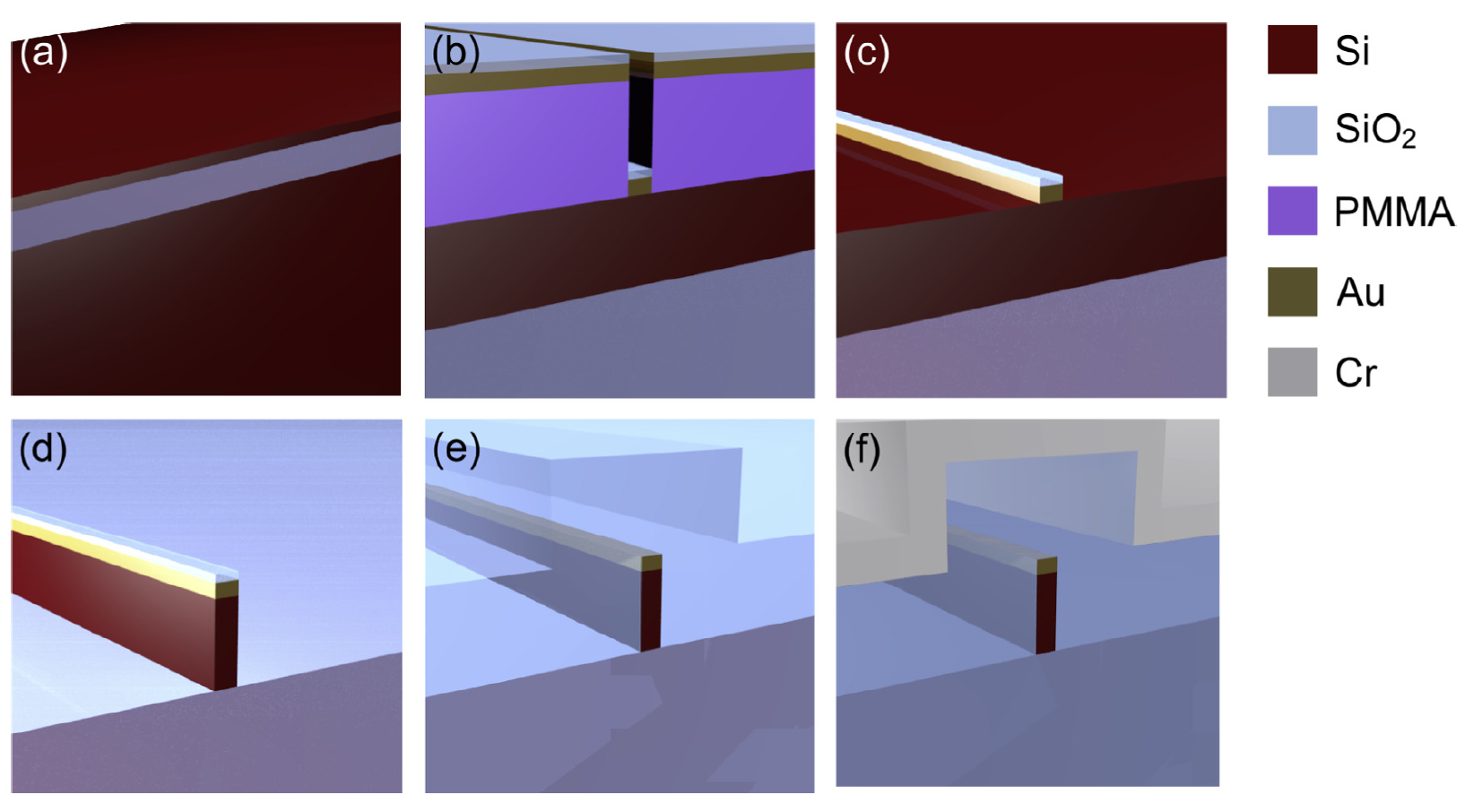
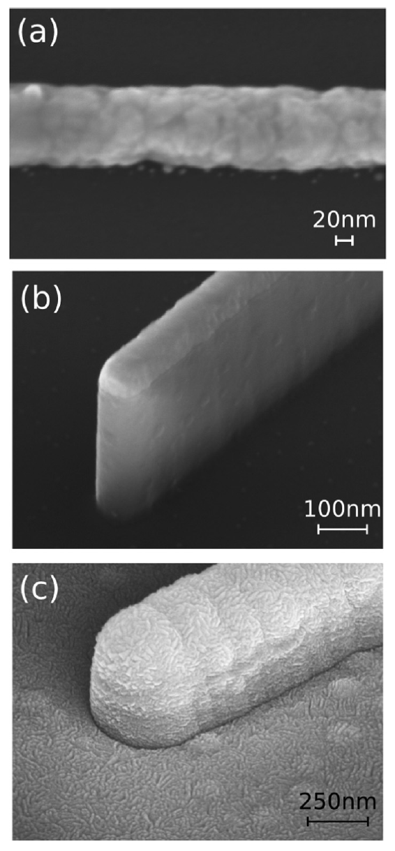
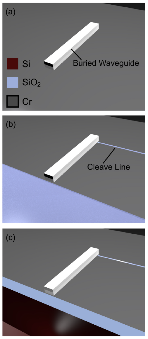
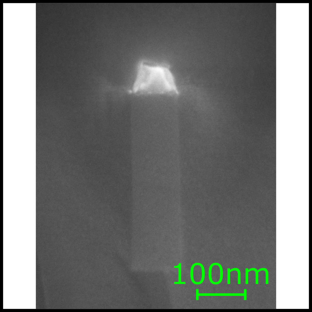
Silicon-loaded nanoplasmonic waveguides were integrated onto a micron-scale characterization beam to allow for accurate and efficient nonlinear optical characterization. The waveguides consist of a 95 nm × 340 nm silicon core that is capped by a 60 nm thick gold film. The characterization beam is formed by precision cleaving one waveguide end facet and by deep silicon etching the substrate area adjacent to the other end facet. This configuration allows input radiation to be coupled directly to the waveguides using a microscope objective and output radiation to be out-coupled with a lensed single-mode optical fiber. The fabrication steps are characterized via scanning electron microscopy at various points throughout the process. The fabricated devices are optically characterized using an ultrafast nonlinear pump-probe time-domain spectroscopy setup. Ultrafast all-optical modulation is measured in the waveguides on two timescales: τ1 = 1.98 ± 0.40 ps and τ2 = 17.9 ± 6.8 ps.