
Introduction

Figure 1: Layout of a standard PolyMUMPS bonding pad design (100um x 100um).
This cell implements the a bonding pad. The first variant implements the standard bonding pad recommended by in the PolyMUMPs® handbook. The second variant implements a substrate bonding pad.
The design of bonding pads is specified in the design handbook for PolyMUMPs [1].
The failure to heed enclosure rules when designing probe pads can result in a number of problems. Some users have experienced shorting of their devices to the substrate as a result of thinned or breached Nitride directly adjacent to pads. If the POLY0 is used for routing and the ANCHOR1 holes are not enclosed by POLY1, the POLY0 line will be cut by the POLY1 etch. To avoid these and other problems, the standard pad shown in figure 2.20, should be used.
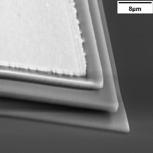
Figure 2: SEM of the corner of a standard PolyMUMPs bonding pad.
Model 1: Standard PolyMUMPS bonding pad design (100 um x 100 um).
Theory
Exclusion Zone
During the bonding process, significant stresses are created. These stresses are not confined to the bonding pad itself, and are known to cause delamination and cracking of nearby structures. A region surrounding bonding pad where these negative effects occur is known as the exclusion zone. The standard bonding pad has an option to mark the exclusion zone.
Obviously, electrical contacts are necessary. Some types of structures must therefore exist in the exclusion zone. The connecting structures must be designed to withstand the stresses creating during bonding. In particular, the standard conducting line is designed so that it can be used within the exclusion zone.
Parasitic Capacitor
Bonding pads are connected to the silicon substrate through a parasitic capacitor. The substrate is conductive, so electrical signals can applied to the pad structure may couple to other nearby structures, including other pads. The documentation on capacitor parameterized cells discusses this in more detail.
This is obviously not a major concern for substrate pads. These pads are designed to intentially breach the silicon nitride layer to make electrical contact with the substrate.
Parameters
Any parameter may be modified, if necessary, to meet design rules. Typically, this involves increasing parameters that specify distances, so that minimum line width and minimum line spacing rules will not be violated. This has been extended to the convention of specifying a zero for some parameters to obtain an instance of the minimum size.
In addition to the parameters listed below, several technology parameters also influence the implementation of parameterized cells. This data must be present in the technology library.
| Name | Description | Range | Units | Poly | Sub |
|---|---|---|---|---|---|
| width | This is the width of the METAL region of the pad. The outer boundary of the cell will be larger. | [0,∞) | um | + | + |
| height | This is the height of the METAL region of the pad. The outer boundary of the cell will be larger. | [0,∞) | um | + | + |
| chamfer | This is the length along each corner that will be chopped. Typically, this parameter should is zero. However, it can be increased to reduced spurious DRC violations in non-manhattan geometries. | [0,∞) | um | + | + |
| include C | If true, then the cell calculates an estimate for the substrate capacitance based on nominal MUMPS parameters. The estimate will then be displayed using the TMP layer during design. | true/false | - | + | - |
| include exclusion | If true, then the cell also shows the extent of the exclusion zone using a circle displayed with the TMP layer. Structures in the exclusion zone may crack and/or delaminate during bonding. | true/false | - | + | - |
| include metal | If true, then metal is placed on top of the pad. Otherwise, the pads are composed solely of poly-silicon. | true/false | - | + | - |
