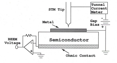
BEEM
Requirements: Samples consist of a buried interface between a conducting surface layer (usually a metal) and a semiconductor. The surface layer must maintain a tunneling current as in any scanning tunneling microscopy (STM) experiment. In addition, its thickness must not exceed the carrier mean free path for 1 - 2 V electrons or holes (eg. 9 nm in Au for electrons). Ballistic electrons are collected by a 3rd ohmic contact (often to the bottom of the semiconductor) with the signal amplified by a high gain op-amp. The diode zero bias resistance must be sufficiently large (> 100 kohms) that the leakage current through the entire diode is not greater than that of the STM injection (nA).
Review article: W. Yi, A.J. Stollenwerk, V. Narayanamurti, Surface Science Reports 64 (2009) 169.
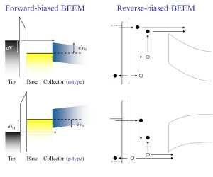
BEEM schematics and band diagrams