
Introduction
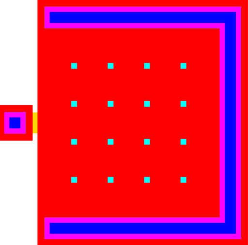
Figure 1: Layout of a parallel-plate capacitor using the structural layers POLY0 and POLY1.
A simple design for a parallel-plate capacitor. The capacitor uses the structural layers POLY0 and POLY1, or the substrate and POLY0. Etch holes may or may not be placed in the POLY1 plate.
Model 1: parallel-plate capacitor using the structural layers POLY0 and POLY1.
Theory
Capacitance
At least to first approximation, the capacitance of the device can be determined using the formula for parallel plate capacitors:
Where, C is the capacitance, ε0 is the permittivity of free space, εr is the relative permittivity of the material, A is the area of the capacitor, w is the capacitor width as specified in the parameters, h is the capacitor height as specified in the parameters, and d is the separation distance between the plates. The value of e can easily be obtained, as it is a fundamental constant. The area can be taken from the device parameters.
The above forumla is limited in that it does not account for fringe effects. In general, the effects of fringing for parallel plate capacitors can be neglected as long as both the width and height of the capacitor are significantly larger then the plate separation, a condition that is easily achieved here. However, the presence of etch holes contributes additional fringing that will always be present as their presence increase along with the area of the capacitor.
POLY0-POLY1 Capacitors
For the POLY0-POLY1 capacitors, the value of d is fixed by the PolyMUMPs® process, and is the equal to the thickness of SOX1, which is 2um. The relative permittivity depends on wheter etch holes are present or not. If present, the intervening material is air (er=1). Otherwise, the intervenining material is mostly silicon dioxide (er=3.7).
Even though this is a capacitor between the POLY0 and POLY1 plates, this design contains a parasitic capacitance that connects the POLY1 plate to the silicon substrate. The substrate is conductive, and so electrical signals can feed into the substrate to other capacitors (both POLY0 and POLY1 capacitors), as well as bonding bads, etc.
Substrate-POLY0 Capacitors
These capacitors are actually between the POLY0 and the silicon substrate. The value of d is equal to the nitride thickness, which is 0.6um. The relative permittivity is that of silicon nitride, and is er=7.5.
Please note that the substrate is highly conductive and so all connections to the substrate should be considered to be electrically connected. Use this capacitor only if one connection can be used as ground. Use the pin connected to the nitride breach ring as ground.
Parasitic Resistance
There are two paths of parasitic conduction between the capacitor's electrodes: bulk conduction through the air and surface conduction over the silicon nitride.
The resistance due to bulk conduction through the air can be calculated through the well known equation for resistance, as follows.
Above, Rair is the parasitic resistance through air, ϊ is the resistivity of air, L is the length of the resistor, and A is the area of the resistor. For the capacitor, this leads to the right-most equation, where d is the separation between the plates, and w and h are parameters provided to the cell.
From [1], the resistivity of air is between 2×10¹³Ωm and 4×10¹³Ωm. For a capacitor with the default width and height of 100um, the restance Rair is between 4×10¹⁵Ω and 8×10¹⁵Ω.
The surface conduction along the silicon nitride surface is easily determined using the following formula:
Above, RSiN is the resistance of the silicon nitride surface, ρ is the surface resistance of the silicon nitride in Ohm/square, L is the minimum spacing between POLY0 and ANCHOR1, P is the capacitor perimeter, w is the capacitor's width as specified in the parameters, and h is the capacitor's height as specified in the parameters.
From the design handbook [2], the POLY0 to ANCHOR1 minimum spacing is 4um. The surface resitance of silicon nitride is on the order of 1012 to 1015Ω [3]. A capacitor with the standard the default width and height of 100um will have a RSiN of 3.4GΩ to 3.4TΩ.
Snap Through
Extremely large POLY0-POLY1 capacitors will be susceptible to snap through. When a voltage is applied across the capacitor, the electro-static forces will create an attraction between the two plates. While the POLY0 plate is completely fixed to the substrate, the POLY1 plate is only supported along three sides. With sufficient electro-static attraction, it will begin to bow toward the POLY0.
When the POLY1 bows, the capacitance will increase.
More important for the phenomena of snap-through, though, is that the electric field strength is increased in the region where the POLY0 and POLY1 are closer. This can lead to increase bowing, leading in turn to increased field strength. At a critical voltage, this process will lead to a run-away process that pulls the POLY1 into contact with the POLY0, shorting the two plates.
This process could be, in part, prevented by not placing etch holes in POLY1. The silicon dioxide present between the two plate would provide some level of structural support. This would, however, seriously complicate determining the capacitance of the device.
Parameters
Any parameter may be modified, if necessary, to meet design rules. Typically, this involves increasing parameters that specify distances, so that minimum line width and minimum line spacing rules will not be violated. This has been extended to the convention of specifying a zero for some parameters to obtain an instance of the minimum size.
In addition to the parameters listed below, several technology parameters also influence the implementation of parameterized cells. This data must be present in the technology library.
| Name | Description | Range | Units | P0 | P1 |
|---|---|---|---|---|---|
| width | This is the width of the capacitor. It does not include the conducting line that goes along the right edge or the pin connected on the left. | [0,∞) | um | + | + |
| height | This is the height of the capacitor. It does not include the conducting lines that go along the top and bottom edges. | [0,∞) | um | + | + |
| pin size | The side length of the terminal. Please refer to the pin parameterized cell. | [0,∞) | um | + | + |
| include C | If this box is checked, then the cell calculates an estimate for the capacitance based on nominal MUMPS parameters. The estimate will then be displayed using the TMP layer during design. | true/false | - | + | + |
| include etch holes | If this box is checked, then the cell automatically places etch hole in the POLY1 layer using data from the technology file. If unchecked, no etch holes will be placed, meaning that the silicon dioxide may not be completely removed from between the plate. Since silicon dioxide has a relative permittivity of ~3.7, this will increase the capacitance. However, the exact increase will be unpredictable since it will depend on how much silicon dioxide remains. | true/false | - | - | + |
References
[1] David R. Lide (editor). CRC Handbook on Chemistry and Physics. CRC Press, London, 1997.
