
Introduction
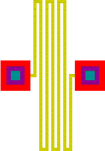
Figure 1: Layout for a snake resistor.
This cell implements a simple resistor. The resistor is a serpetine length of minimum width POLY0.
Theory
The resistance between the terminals can be calculated using the following formula:
Where, R is the resistance between terminals, b is the number POLY0 bars, l is the length of each bar in the POLY0 snake, g is the distance separating the bars, w is the width of each bar, and R□ is the resistance per square of the POLY0 thin film.
This cell does not currently allow the values of w to be specified. Instead, this parameter is set to the minimum line width as stored in the technology file.
The resistance per square can be calculated by using the following formula:
The values for ρ and t are process dependent, and can vary from process run to process run. However, for the PolyMUMPs® process they have nominal values of 0.5um for t [1] and 1.3×10⁻³Ωcm. With the default parameters, the resistance should be approximately 7969Ω.
Parameters
Any parameter may be modified, if necessary, to meet design rules. Typically, this involves increasing parameters that specify distances, so that minimum line width and minimum line spacing rules will not be violated. This has been extended to the convention of specifying a zero for some parameters to obtain an instance of the minimum size.
In addition to the parameters listed below, several technology parameters also influence the implementation of parameterized cells. This data must be present in the technology library.
| Name | Description | Range | Units |
|---|---|---|---|
| width | This parameter specifies the total width of each bear within the resistor snake. | [0,∞) | um |
| bars | The number of complete bars to include. Even is this parameter is zero, there will be two have bars present. | [0,∞) | - |
| gap | The amount of space between bars. The parameter will be increased if necessary so that it is at least the POLY0 minimum spacing. | [0,∞) | um |
| pin size | At each end of the resistor is a pin. This parameter controls the side length of the pins. More details are available in the documentation for the pin parameterized cell. | [0,∞) | um |
| chamfer | This is the length along each corner that will be chopped. Typically, this parameter should is zero. However, it can be increased to reduced spurious DRC violations in non-manhattan geometries. | [0,∞) | um |
| include R | If this box is checked, the pcell will calculate the resistance of the device using standard MUMPS parameters (as above) and display the value using the TMP layer. | true/false | - |
